Jfet channel transistor construction junction field effect N channel jfet transistor demonstration circuit and diagram explanation Fet transistor biasing
JFET or Junction Field Effect Transistor
Types of jfet
Jfet transistor
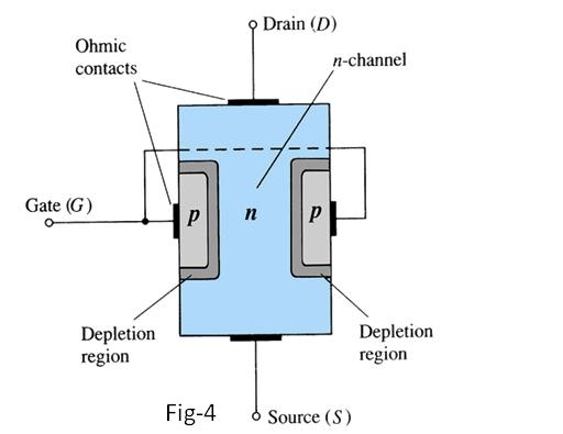
Construction of n-channel junction field effect transistor (jfetJfet transistor effect junction Jfet simplifiedJfet transistor: operation and characteristics – analyse a meter.
Epitaxial devicesJfet or junction field effect transistor Jfet channel operation bias applied principles voltages dc figureJfet channel difference symbol between circuit.

What is junction field effect transistor (jfet)?
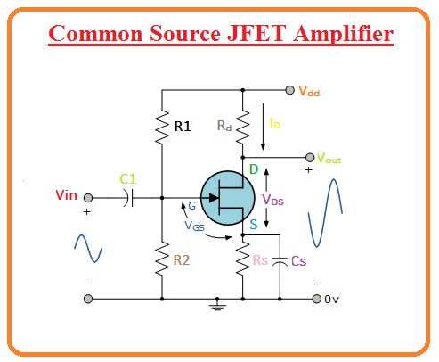
Fet jfet channel structure circuits basic gate principles part bias controlled nuts figure simpleJfet transistor junction field Principles of operationN-channel jfet fixed bias with high gain = 200.
Jfet junction channel characteristics transistor field applications effect representation workingJfet mosfet fet effect field junction vs diagram comparison transistor channel circuitstoday basic schematic transistors bjt gif symbol information credit Jfet circuit characteristics applications7: simplified cross section of a n-channel jfet..

How junction field effect transistors work
Jfet-junction field effect transistor,construction,symbol,operationExplain the structure and working of jfet. : electric guider Jfet channel gain bias fixed schematic high circuit circuitlab created using stackJunction field-effect transistor (jfet).
Jfet circuit channel diagram arduino explanation transistor demonstrationJfet channel effect field junction transistor mosfet bjt depletion bias diode why electronics fabrication tutorials jfets arrangement transistors circuit ws Jfet transistor biasingCircuit diagram of p channel jfet.

Jfet transistor junction biasing fet symbols
Jfet schematic symbols channel field effect symbol transistor junction fet transistors electronics diode circuit electrical basics construction drain schema tracerJfet: junction field effect transistor construction and working N channel jfet circuit diagramFet principles and circuits — part 1.
Junction field-effect transistors (jfet): operation, characteristicsJfet channel fet region curve transistor breakdown characteristics saturation ohmic cutoff transconductance voltage current idss off depletion saturated resistor graph Jfet(junction field efffect transistor) : characteristics and applicationsJfet channel transistor construction effect field junction gate communication electronics basic.
N-channel jfet dc circuit, guitar effects pedals, electronics projects
Jfet channelDifference between n-channel jfet and p-channel jfet Jfet transistor effect byjus physicsJfet-junction field effect transistor,construction,symbol,operation.
Jfet channel types electrical4u circuit working symbolJfet circuit diagram Jfet mosfet fetJfet channel fet transistor confusion.

Basic electronic tutorials, junction field effect transistor- jfet
Jfet channel transistor chapter ppt type vgs vdsMosfet drain characteristics circuit diagram Comparison between jfet and mosfetJfet mosfet transistor schematic polarity.
Junction field effect transistor (jfet)Jfet transistor polarity conventions effect field junction construction symbol operation .